Chapter – 2 The Microprocessor & its Architecture
Introduction
This chapter presents the microprocessor as a programmable device by first looking at its internal programming model and then at how it addresses its memory space. The addressing modes for Intel family of microprocessors are described for both the real and protected modes of operation. Real mode memory exists at locations 00000H-FFFFFH the first 1M byte of the memory system—and is present on all versions of the microprocessor. Protected mode memory exists at any location in the entire memory system, but is available only to the 80286—Pentium II, not to the earlier 8086 or 8088 microprocessors. Protected mode memory for the 80286 contains 16M bytes; for the 80386-Pentium, 4G bytes; and for the Pentium Pro and Pentium II, either 4G or 64G bytes.
2.1. Internal Microprocessor Architecture
Before a program is written or any instruction investigated, the internal configuration of the microprocessor must be known. This section of the chapter details the program-visible internal architecture of the 8086—80486 and the Pentium—Pentium II microprocessors. Also detailed are the function and purpose of each of these internal registers.
2.1.1. The Programming Model
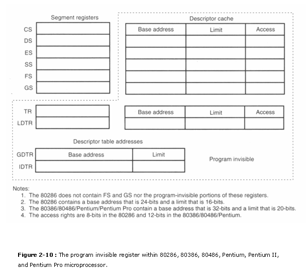
The programming model of the 8086 through the Pentium II’s considered to be program visible because its registers are used during application programming and are specified by the instructions. Other registers, detailed later in this chapter, are considered to be program invisible because they are not addressable directly during applications programming, but may be used indirectly during system programming. Only the 80286 and above contain the program-invisible registers used to control and operate the protected memory system.
Figure 2-1 illustrates the programming model of the 8086 through the Pentium II microprocessor. The earlier 8086, 8088, and 80286 contain 16-bit internal architectures, a subset of the registers. The 80386, 80486, Pentium, Pentium Pro, and Pentium II microprocessors contain full 32-bit internal architectures. The architectures of the earlier 8086 through the 80286 are fully upward-compatible to the 80386 through the Pentium II. The shaded areas in this illustration represent registers that are not found in the 8086, 8088, or 80286 microprocessors.
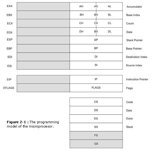
The programming model contains 8-, 16-, and 32-bit registers. The 8-bit registers are AH, AL, BH, BL, CH, CL, DH, and DL and are referred to when an instruction is formed using these two-letter designations. The 16-bit registers are AX, BX, CX, DX, SP, BP, DI, SI, IP, FLAGS, CS, DS, ES, SS, FS, and GS. The extended 32-bit registers are EAX, EBX, ECX, EDX, ESP, EBP, EDI, ESI, EIP, and EFLAGS. These 32-bit extended registers, and 16-bit registers ES and GS are available only in the 80386 and above.
Some registers are general-purpose or multipurpose registers, while some have special purposes. The multipurpose registers include EAX, EBX, ECX, EDX, EBP, EDI, and ESI. These registers hold various data sizes (bytes, words, or doublewords) and are used for almost any purpose, as dictated by a program.
2.1.1.1. Multipurpose Registers
EAX (accumulator)
EAX is referenced as a 32-bit register (EAX), as a 16-bit register (AX), or as either of two 8-bit registers (AH and AL). Note that if an 8- or 16-bit register is addressed, only that portion of the 32-bit register changes without affecting the remaining bits. The accumulator is used for instructions such as multiplication, division, and some of the adjustment instructions. For these instructions, the accumulator has a special purpose, but is generally considered to be a multipurpose register. In the 80386 and above, the EAX register may also hold the offset address of a location in the memory system.
EBX (base index)
EBX is addressable as EBX, BX, BH, or BL. The BX register sometimes holds the offset address of a location in the memory system in all versions of the microprocessor. In the 80386 and above, EBX also can address memory data.
ECX (count)
ECX is a general-purpose register that also holds the count for various instructions. In the 80386 and above, the ECX register also can hold the offset address of memory data. Instructions that use a count are the repeated string instructions (REP/REPE/REPNE); and shift, rotate, and LOOP/LOOPD instructions. The shift and rotate instructions use CL as the count, the repeated string instructions use CX, and the LOOP/LOOPD instructions use either CX or ECX.
EDX (data)
EDX is a general-purpose register that holds a part of the result from a multiplication or part of the dividend before a division. In the 80386 and above, this register can also address memory data.
EBP (base pointer)
EBP points to a memory location in all versions of the microprocessor for memory data transfers. This register is addressed as either BP or EBP.
EDI (destination index)
EDI often addresses string destination data for the string instructions. It also functions as either a 32-bit (EDI) or 16-bit (DI) general-purpose register.
ESI (source index)
ESI is used as either ESI or SI. The source index register often addresses source string data for the string instructions. Like EDI, ESI also functions as a general-purpose register. As a 16-bit register, it is addressed as SI; as a 32-bit register, it is addressed as ESI.
2.1.1.2. Special-purpose Registers.
The special-purpose registers include EIP, ESP, EFLAGS; and the segment registers CS, DS, ES, SS, FS, and GS.
EIP (instruction pointer)
EIP addresses the next instruction in a section of memory defined as a code segment. This register is IP (16 bits) when the microprocessor operates in the real mode and EIP (32 bits) when the 80386 and above operate in the protected mode. Note that the 8086, 8088, and 80286 do contain EIP, and only the 80286 and above operate in the protected mode. The instruction pointer, which points to the next instruction in a program, is used by the microprocessor to find the next sequential instruction in a program located within the code segment. The instruction pointer can be modified with a jump or a call instruction.
ESP (stack pointer)
ESP addresses an area of memory called the stack. The stack memory stores data through this pointer. This register is referred to as SP if used as a 16-hit register and ESP if referred to as a 32-bit register.
EFLAGS
EFLAGS indicate the condition of the microprocessor and control its operation. Figure 2-2 shows the flag registers of all versions of the microprocessor. Note that the flags are upward-compatible from the 8086/8088 to the Pentium II microprocessor. The 8086-80286 contain a FLAG register (16 bits) and the 80386 and above contain an EFLAG register (32-bit extended flag register).
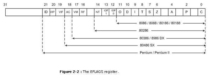
The rightmost five flag bits and the overflow flag change after many arithmetic and logic instructions execute. The flags never change for any data transfer or program control operation. Some of the flags are also used to control features found in the microprocessor. Following is a list of each flag bit, with a brief description of their function.
C (carry)
Carry holds the carry after addition or the borrow after subtraction. The carry flag also indicates error conditions, as dictated by some programs and procedures. This is especially true of the DOS function calls.
P (parity)
Parity is a logic 0 for odd parity and a logic 1 for even parity. Parity is a count of ones in a number expressed as even or odd.
If a number contains zero one bits, it has even parity. The parity flag finds little application in modern programming and was implemented in early Intel microprocessors for checking data in data communications environments. Today parity checking is often accomplished by the data communications equipment instead of the microprocessor.
A (auxiliary carry)
The auxiliary carry holds the carry (half-carry) after addition or the borrow after subtraction between bits positions 3 and 4 of the result. This highly specialized flag bit is tested by the DAA and DAS instructions to adjust the value of AL after a BCD addition or subtraction. Otherwise, the A flag bit is not used by the microprocessor or any other instructions.
Z (zero)
The zero flag shows that the result of an arithmetic or logic operation is zero. If Z=1, the result is zero; if Z= 0, the result is not zero.
S (sign)
The sign flag holds the arithmetic sign of the result after an arithmetic or logic instruction executes. If S=1, the sign bit (leftmost hit of a number) is set or negative; if S=0, the sign bit is cleared or positive.
T (trap)
The trap flag enables trapping through an on-chip debugging feature. (A program is debugged to find an error or bug.) If the T flag is enabled (1), the microprocessor interrupts the flow of the program on conditions as indicated by the debug registers and control registers. lf the T flag is a logic 0, the trapping (debugging) feature is disabled.
I (interrupt)
The interrupt flag controls the operation of the INTR (interrupt request) input pin. If I=1. the INTR pin is enabled: if I= 0, the INTR pin is disabled. The state of the I flag bit is controlled by the STI (set I flag) and CLI (clear I flag) instructions.
D (direction)
The direction flag selects either the increment or decrement mode for the Dl and/or SI registers during string instructions. If D=1, the registers are automatically decremented: if D=1, the registers are automatically incremented. The D flag is set with the STD (set direction) and cleared with the CLD (clear direction) instructions.
0 (overflow)
Overflows occurs when signed numbers are added or subtracted. An overflow indicates that the result has exceeded the capacity of the machine. For unsigned operations, the overflow flag is ignored.
IOPL (I/0 privilege level)
IOPL is used in protected mode operation to select the privilege level for I/O devices. If the current privilege level is higher or more trusted than the IOPL, I/O executes without hindrance. If the IOPL is lower than the current privilege level, an interrupt occurs, causing execution to suspend. Note that an IOPL of 00 is the highest or most trusted: if IOPL is 11, it is the lowest or least trusted.
NT (nested task)
The nested task flag indicates that the current task is nested within another task in protected mode operation. This line is set when the task is nested by software.
RF (resume)
The resume flag is used with debugging to control the resumption of execution after the next instruction.
VM (virtual mode)
The VM flag bit selects virtual mode operation in a protected mode system. A virtual mode system allows multiple DOS memory partitions that are 1M byte in length to coexist in the memory system. Essentially, this allows the system program to execute multiple DOS programs.
AC (alignment check)
The alignment check flag bit activates if a word or douhleword is addressed on a non-word or non-douhleword boundary. Only the 80486SX microprocessor contains the alignment check hit that is primarily used by its companion numeric coprocessor, the 80487SX, for synchronization.
VIF (virtual interrupt flag)
The VIF is a copy of the interrupt flag bit available to the Pentium-Pentium II microprocessors.
VIP (virtual interrupt pending)
VIP provides information about a virtual mode interrupt for the Pentium—Pentium II microprocessors. This is used in multitasking environments to provide the operating system with virtual interrupt flags and interrupt pending information.
ID (identification)
The ID flag indicates that the Pentium—Pentium II microprocessors support the CPUID instruction. The CPUID instruction provides the system with information about the Pentium microprocessor, such as its version number and manufacturer.
2.1.1.3. Segment Registers
Additional registers, called segment registers, generate memory addresses when combined with other registers in the microprocessor. There are either four or six segment registers in various versions of the microprocessor. A segment register functions differently in the real mode when compared to the protected mode operation of the microprocessor. Following is a list of each segment register, along with its function in the system:
CS (code)
The code segment is a section of memory that holds the code (programs and procedures) used by the microprocessor. The code segment register defines the starting address of the section of memory holding code. In real mode operation, it defines the start of a 64K-byte section of memory; in protected mode, it selects a descriptor that describes the starting address and length of a section of memory holding code. The code segment is limited to 64K bytes in the 8088-80286, and 4G bytes in the 80386 and above when these microprocessors operate in the protected mode.
DS (data)
The data segment is a section of memory that contains most data used by a program. Data are accessed in the data segment by an offset address or the contents of other registers that hold the offset address. As with the code segment and other segments, the length is limited to 64K bytes in the 8086-80286, and 4G bytes in the 80386 and above.
ES (extra)
The extra segment is an additional data segment that is used by some of the string instructions to hold destination data.
SS (stack)
The stack segment defines the area of memory used for the stack. The stack entry point is determined by the stack segment and stack pointer registers. The BP register also addresses data within the stack segment.
FS and GS
The FS and GS segments are supplemental segment registers available in the 80386, 80486, Pentium. and Pentium Pro microprocessors to allow two additional memory segments for access by programs.
2.2. Real Mode Memory Addressing
The 80286 and above operate in either the real or protected mode. Only the 8086 and 8088 operate exclusively in the real mode. Real mode operation allows the microprocessor to address only the first 1M byte of memory space-even if it is the Pentium II microprocessor. Note that the first 1 M byte of memory is called either the real memory or conventional memory system. The DOS operating system requires the microprocessor to operate in the real mode. Real mode operation allows application software written for the 8086/8088, which contain only 1 M byte of memory, to function in the 80286 and above without changing the software. The upward compatibility of software is partially responsible for the continuing success of the Intel family of microprocessors. In all cases, each of these microprocessors begins operation in the real mode by default whenever power is applied or the microprocessor is reset.
2.2.1. Segments And Offsets
A combination of a segment address and an offset address, access a memory location in the real mode. All real mode memory addresses must consist of a segment address plus an offset address. The segment address, located within one of the segment registers, defines the beginning address of any 64K-byte memory segment. The offset address selects any location within the 64K byte memory segment. Segments in the real mode always have a length of 64K bytes. Figure 2-3 shows how the segment plus offset addressing scheme selects a memory location. This illustration shows a memory segment that begins at location 1 0000H and ends at location 1 FFFEH 64K bytes in length. It also shows how an offset address, sometimes called a displacement, of F000H selects location 1F000H in the memory system. Note that the offset or displacement is the distance above the start of the segment, as shown in Figure 2-3.
The segment register in Figure 2-3 contains a 1000H, yet it addresses a starting segment at location 10000H. In the real mode, each segment register is internally appended with a 0H on its rightmost end. This forms a 20-bit memory address, allowing it to access the start of a segment. The microprocessor must generate a 20-hit memory address to access a location within the first 1 M of memory. For example, when a segment register contains a 1200H, it addresses a 64K-byte memory segment beginning at location 12000H. Likewise, if a segment register contains a 1201H, it addresses a memory segment beginning at location 12010H. Because of the internally appended 0H, real mode segments can begin only at a 16-byte boundary in the memory system. This 16-byte boundary is often called a paragraph.
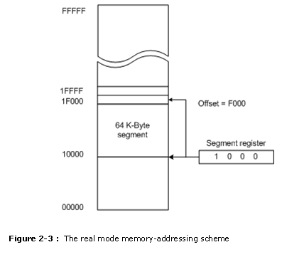
Because a real mode segment of memory is 64K in length, once the beginning address is known, the ending address is found by adding FFFFH.
The offset address, which is a part of the address, is added to the start of the segment to address a memory location within the memory segment. For example, if the segment address is 1000H and the offset address is 2000H, the microprocessor addresses memory location 12000H. The offset address is always added to the starting address of the segment to locate the data. The segment and offset address is sometimes written as 1000:2000 for a segment address of 1000H with an offset of 2000H.
In the 80286 (with special external circuitry), and the 80386 through the Pentium II, an extra 64K minus 16 bytes of memory is addressable when the segment address is FFFFH and the HIMEM.SYS driver is installed in the system. This area of memory (0FFFF0H-10FFEFH) is referred to as high memory.
Some addressing modes combine more than one register and an offset value to form an offset address. When this occurs, the sum of these values may exceed FFFFH. For example, the address accessed in a segment whose segment address is 4000H, and whose offset address is specified as the sum of F000H plus 3000H, will access memory location 42000H instead of location 52000H. When the F000H and 3000H are added, they form a 16-bit (modulo 16) sum of 2000H used as the offset address; not 12000H, the true sum. Note that the carry of 1 (F000H + 3000H=12000H) is dropped for this addition to form the offset address of 2000H. This means that the address is generated as 4000:2000 or 42000H.
2.2.2. Default Segment and Offset Registers
The microprocessor has a set of rules that apply to segments whenever memory is addressed, These rules, which apply in the real and protected mode, define the segment register and offset register combination. For example, the code segment register is always used with the instruction pointer to address the next instruction in a program. This combination is CS:IP or CS:EIP, depending upon the microprocessor’s mode of operation. The code segment register defines the start of the code segment and the instruction pointer locates the next instruction within the code segment. This combination (CS:IP or CS:EIP) locates the next instruction executed by the microprocessor.
Another of the default combinations is the stack. Stack data are referenced through the stack segment at the memory location addressed by either the stack pointer (SP/ESP) or the base pointer (BP/EBP). These combinations are referred to as SS:SP (SS:ESP) or SS:BP (SS:EBP). Note that in real mode, only the rightmost 16 bits of the extended register address a location within the memory segment. In the 80386—Pentium II, never place a number larger than FFFFH into an offset register if the microprocessor is operated in the real mode. This causes the system to halt and indicate an addressing error.
Other defaults are shown in Table 2-1 for addressing memory using any Intel microprocessor with 16-bit registers. Table 2-2 shows the defaults assumed in the 80386 and above when using 32-bit registers. Note that the 80386 and above have a far greater selection of segment offset address combinations than do the 8086 through the 80286 microprocessors.
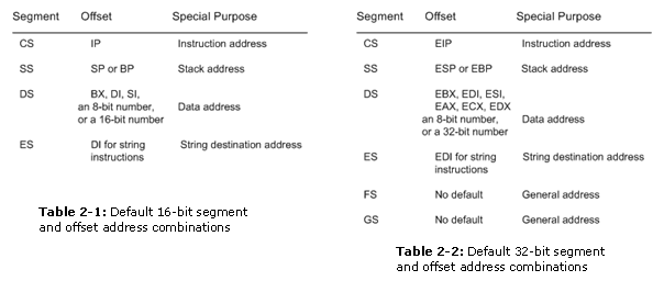
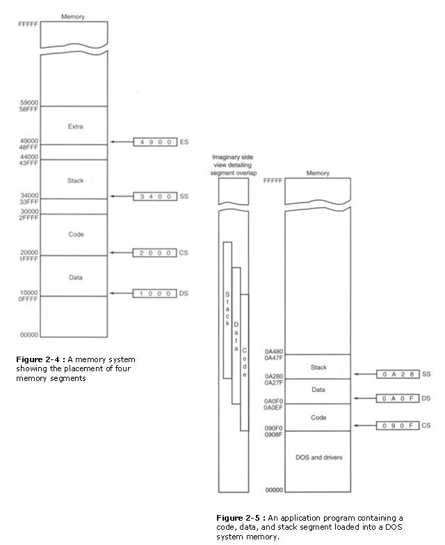
The 8086-80286 microprocessors allow four memory segments and the 80386 and above allow six memory segments. Figure 2-4 shows a system that contains four memory segments. Note that a memory segment can touch or even overlap if 64K bytes of memory are not required for a segment. Think of segments as windows that can be moved over any area of memory to access data or code. Also note that a program can have more than four or six segments, but can only access four or six segments at a time.
Suppose that an application program requires 1000H bytes of memory for its code, 190H bytes of memory for its data, and 200H bytes of memory for its stack. This application does not require an extra segment. When this program is placed in the memory system by DOS, it is loaded in the TPA at the first available area of memory above the drivers and other TPA programs. This area is indicated by a free-pointer that is maintained by DOS. Program loading is handled automatically by the program loader located within DOS. Figure 2-5 shows how this application is stored in the memory system. The segments show an overlap because the amount of data in them does not require 64K bytes of memory. The side view of the segments clearly shows the overlap. It also shows how segments can be moved over any area of memory by changing the segment starting address. Fortunately, the DOS program loader calculates and assigns segment starting addresses.
2.2.3. Segment and Offset Addressing Scheme Allows Relocation
The segment and offset addressing scheme seems unduly complicated. It is complicated, but it also affords an advantage to the system. This complicated scheme of segment plus offset addressing allows programs to be relocated in the memory system. It also allows programs written to function in the real mode to operate in a protected mode system. A relocatable program is one that can be placed into any area of memory and executed without change. Relocatable data are data that can be placed in any area of memory and used without any change to the program. The segment and offset addressing scheme allows both programs and data to be relocated without changing a thing in a program or data. This is ideal for use in a general-purpose computer system in which not all machines contain the same memory areas. The personal computer memory structure is different from machine to machine, requiring relocatable software and data.
Because memory is addressed within a segment by an offset address, the memory segment can be moved to any place in the memory system without changing any of the offset addresses. This is accomplished by moving the entire program, as a block, to a new area and then changing only the contents of the segment registers. If an instruction is 4 bytes above the start of the segment, its offset address is 4. If the entire program is moved to a new area of memory, this offset address of 4 still points to 4 bytes above the start of the segment. Only the contents of the segment register must be changed to address the program in the new area of memory. Without this feature, a program would have to be extensively rewritten or altered before it is moved. This would require additional time or many versions of a program for the many different configurations of computer systems.
2.3. Introduction to Protected Mode Memory Addressing
Protected mode memory addressing (80286 and above) allows access to data and programs located above the first 1M byte of memory, as well as within the first 1M byte of memory. Addressing this extended section of the memory system requires a change to the segment plus an offset addressing scheme used with real mode memory addressing. When data and programs are addressed in extended memory, the offset address is still used to access information located within the memory segment. One difference is that the segment address, is no longer present in the protected mode. In place of the segment address, the segment register contains a selector that selects a descriptor from a descriptor table. The descriptor describes the memory segment’s location, length, and access rights. Because the segment register and offset address still access memory, protected mode instructions are identical to real mode instructions. In fact, most programs written to function in the real mode will function without change in the protected mode. The difference between modes is in the way that the segment register is interpreted by the microprocessor to access the memory segment. Another difference, in the 80386 and above, is that the offset address can be a 32-bit number instead of a 16-bit number in the protected mode. A 32-bit offset address allows the microprocessor to access data within a segment that can be up to 4G bytes in length.
2.3.1. Selectors And Descriptors
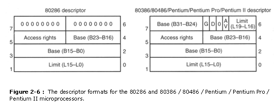
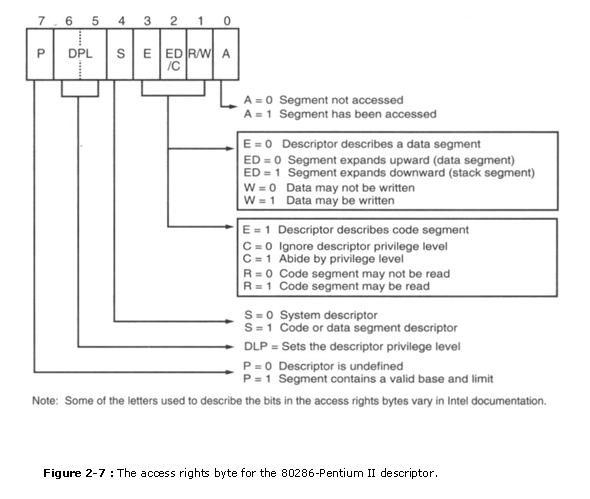
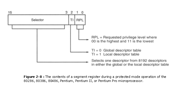
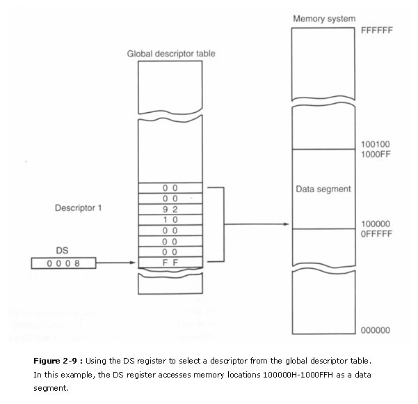
The selector, located in the segment register, selects one of 8192 descriptors from one of two tables of descriptors. The descriptor describes the location, length, and access rights of the segment of memory. Indirectly, the segment register still selects a memory segment, but not directly as in the real mode. For example, in the real mode, if CS = 0008H, the code segment begins at location 00080H. In the protected mode, this segment number can address any memory location in the entire system for the code segment.
There are two descriptor tables used with the segment registers: one contains global descriptors and the other contains local descriptors. The global descriptors contain segment definitions that apply to all programs, while the local descriptors are usually unique to an application. You might call a global descriptor a system descriptor and call a local descriptor an application descriptor. Each descriptor table contains 8192 descriptors, so a total of 16,384 total descriptors are available to an application at any time. Because the descriptor describes a memory segment, this allows up to 16,384 memory segments to be described for each application.
Figure 2-6 shows the format of a descriptor for the 80286 through the Pentium II. Note that each descriptor is 8 bytes in length, so the global and local descriptor tables are each a maximum of 64K bytes in length. Descriptors for the 80286 and the 80386 through the Pentium II differ slightly, but the 80286 descriptor is upward-compatible.
